2 Theoretical Background
This chapter introduces the theory and core concepts necessary for IC design of a biquad filter. It is structured in a way, that it goes from the big picture to the small components. First, biquad filters are introduced with a focus on the universal biquad filter. After that, operational amplifiers come into the the foreground, as biquad filters make use of them in their circuits. Operational amplifiers are looked upon from an IC design standpoint.
2.1 Biquad filter
The biquadratic filter, also known as the biquad filter, has its earliest implementation in the 1960s but is still in use today, most commonly in radio frequency receivers (Razavi 2018). In its application in RF-technology, it is used to remove unwanted neighboring signals ans noise (Razavi 2024). As biquad filter are second-order filters, they are also used as building blocks for higher filter implementations, by cascading them and adding first order filters (Rao and Ravikumar 2012).
2.1.1 Universal biquad filter
For the filter design in this project, an universal biquad filter is used. The universal biquad filter is biquad filter variant with four operational amplifiers used in its design and the property of being able to be used in four different filter variants. Depending on the output of the universal biquad used, a low pass filter, high pass filter, band pass filter, or band stop filter will be implemented. This can be seen in Figure 2.1. (Rao and Ravikumar 2012)
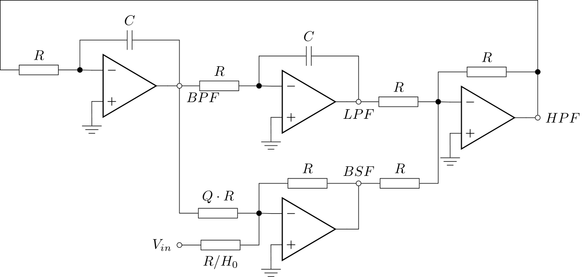
The universal biquad filter consists of two non-inverting amplifiers working as adders in the circuit and two integrators. By setting \(R\) and \(C\) to specific values, the resonance frequency can be chosen. Other parameters adjustable in the universal biquad filter are the quality factor \(Q\) and the low-frequency gain \(H_0\). The quality factor and low-frequency gain determine the frequency response peaks of the low pass filter and the band pass filter. (Rao and Ravikumar 2012)
2.1.2 Characteristics
As the universal biquad filter is a second order filter with the specified outputs low pass, high pass, band pass, and band stop, each filter option can be described with a tranfer function on system level. The general second order transfer function is:
\[ H(s) = \frac{a_1 s^2 + b_1 s + c_1}{a_2 s^2 + b_2 s + c_2} \tag{2.1}\]
The coeffcients can be choosen so, that different responses, like low pass, high pass, band pass, and band stop are achieved.
In filter design a variant of this generalized transfer function is often choosen because it is easier describe the system by quality factor and angular frequency. Equation 2.2 is an exemplatory low pass filter with a transfer function specified for filter design. (Razavi 2018)
\[ H(s) = \frac{\omega_n^2}{s^2 + \frac{\omega_n}{Q} s + \omega_n^2} \tag{2.2}\]
\(Q\) determines amoung other things the amount of peaking the transfer function has at the chosen frequency. Figure 2.2 shows this graphically, the amout of peaking increases with increasing quality factor \(Q\).
Code
# Behavioral Analysis Biquad Filter

import numpy as np
import matplotlib.pyplot as plt

# Initial values
f0 = 1e3  # Resonance frequency in Hz
w0 = 2 * np.pi * f0  # Angular frequency in rad/s
Q1 = 1  # Quality factor
Q2 = 2
Q3 = 5
Q4 = 10
Q5 = 100
H0 = 1  # Play around with this later

# Logarithmic frequency axis
frequencies = np.logspace(2, 4, 10000)  # Frequency from 10^2 to 10^4 Hz
s = 1j * 2 * np.pi * frequencies  # Laplace-Variable s = jω

############################################
# Transfer functions of Active Filters
############################################

### Numerator
# Low Pass Filter
b_lp = H0

# High Pass Filter
#b_hp = (H0 * (s**2 / w0**2))

# Band Pass Filter
#b_bp = (-H0 * (s / w0))

# Band Stop Filter
#b_bs = -((1 + (s**2 / (w0**2))) * H0)

# Denominator -> for all filters the same
a0 = 1
a1_1 = (s / (w0 * Q1))
a1_2 = (s / (w0 * Q2))
a1_3 = (s / (w0 * Q3))
a1_4 = (s / (w0 * Q4))
a1_5 = (s / (w0 * Q5))
a2 = (s**2 / (w0**2))

den1 = a0 + a1_1 + a2
den2 = a0 + a1_2 + a2
den3 = a0 + a1_3 + a2
den4 = a0 + a1_4 + a2
den5 = a0 + a1_5 + a2

############################################
# Calculation of the transfer functions H(s)
############################################
Hs_lp_1 = b_lp / den1
Hs_lp_2 = b_lp / den2
Hs_lp_3 = b_lp / den3
Hs_lp_4 = b_lp / den4
Hs_lp_5 = b_lp / den5
#Hs_hp = b_hp / den
#Hs_bp = b_bp / den
#Hs_bs = b_bs / den

# Bode Diagram
fig, axs = plt.subplots(2)
#fig.suptitle("frequency response of biquad filter")

# Low Pass Filter
axs[0].semilogx(frequencies, 20 * np.log10(np.abs(Hs_lp_1)), label='$Q = 1$')
axs[1].semilogx(frequencies, np.unwrap(np.angle(Hs_lp_1)) * (180 / np.pi), label='$Q = 1$')
axs[0].semilogx(frequencies, 20 * np.log10(np.abs(Hs_lp_2)), label='$Q = 2$')
axs[1].semilogx(frequencies, np.unwrap(np.angle(Hs_lp_2)) * (180 / np.pi), label='$Q = 2$')
axs[0].semilogx(frequencies, 20 * np.log10(np.abs(Hs_lp_3)), label='$Q = 5$')
axs[1].semilogx(frequencies, np.unwrap(np.angle(Hs_lp_3)) * (180 / np.pi), label='$Q = 5$')
axs[0].semilogx(frequencies, 20 * np.log10(np.abs(Hs_lp_4)), label='$Q = 10$')
axs[1].semilogx(frequencies, np.unwrap(np.angle(Hs_lp_4)) * (180 / np.pi), label='$Q = 10$')
axs[0].semilogx(frequencies, 20 * np.log10(np.abs(Hs_lp_5)), label='$Q = 100$')
axs[1].semilogx(frequencies, np.unwrap(np.angle(Hs_lp_5)) * (180 / np.pi), label='$Q = 100$')
'''
# High Pass Filter
axs[0].semilogx(frequencies, 20 * np.log10(np.abs(Hs_hp)), label='high pass')
axs[1].semilogx(frequencies, np.unwrap(np.angle(Hs_hp)) * (180 / np.pi), label='high pass')

# Band Pass Filter
axs[0].semilogx(frequencies, 20 * np.log10(np.abs(Hs_bp)), label='band pass')
axs[1].semilogx(frequencies, np.unwrap(np.angle(Hs_bp)) * (180 / np.pi), label='band pass')

# Band Stop Filter
axs[0].semilogx(frequencies, 20 * np.log10(np.abs(Hs_bs)), label='band stop')
axs[1].semilogx(frequencies, (np.angle(Hs_bs)) * (180 / np.pi), label='band stop')
'''
#axs[0].title("amplitude response")
axs[0].set_xlabel("frequency/Hz")
axs[0].set_ylabel("amplitude/dB")
#axs[0].set_ylim(-50, 25)
axs[0].grid(True, which="both", ls="--")
axs[0].legend(loc=1)

#axs[1].title("phase response")
axs[1].set_xlabel("frequency/Hz")
axs[1].set_ylabel("phase/deg")
axs[1].grid(True, which="both", ls="--")
axs[1].legend()

plt.tight_layout()
#plt.show()

plt.savefig('../images/sec_theorectical_background/lowPassDifferentQ.png', format='png', dpi=1000)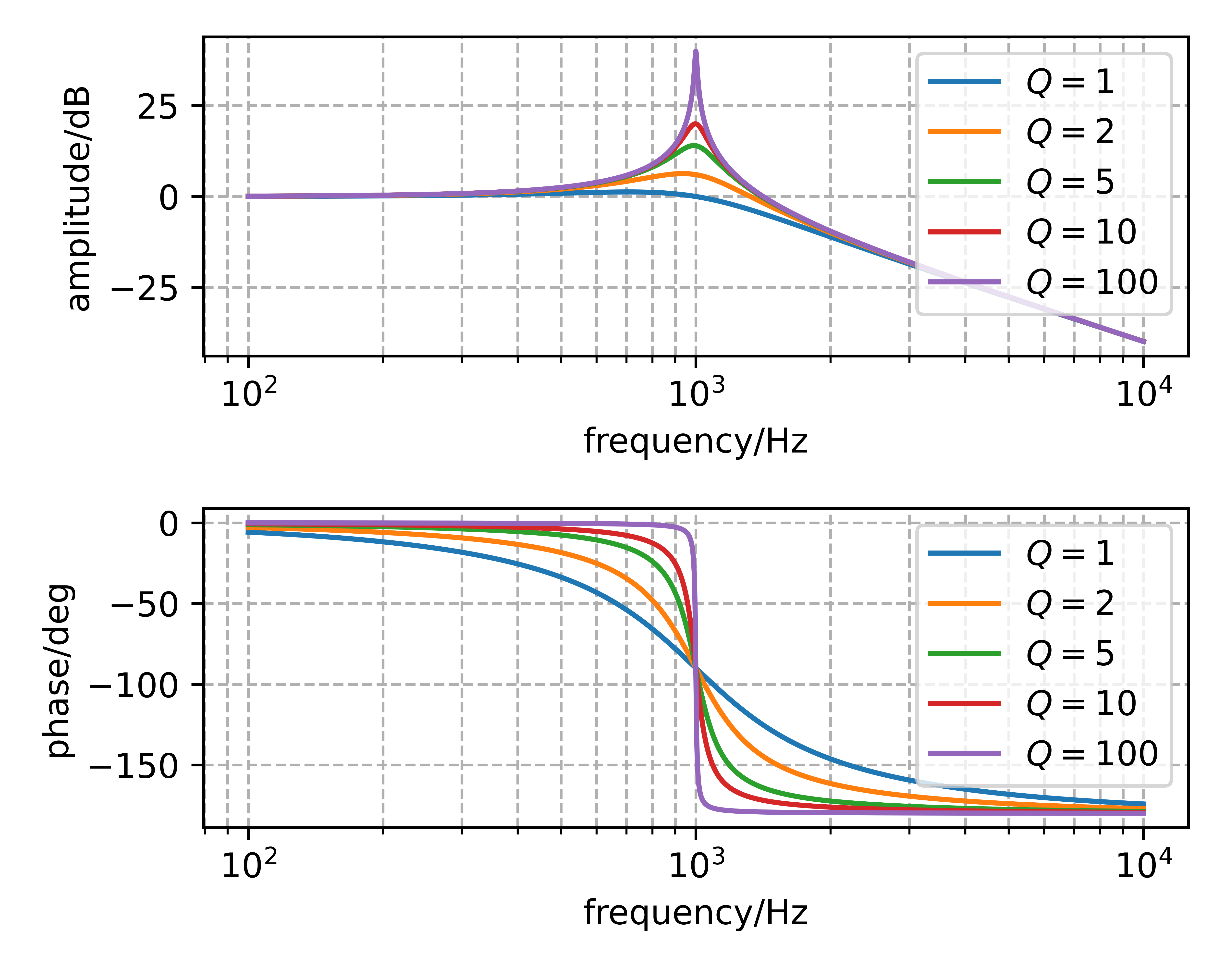
The height of the peak can be calculated with:
\[ A_{peak} = \frac{Q}{\sqrt{1 - \frac{1}{4Q^2}}} \tag{2.3}\]
For \(Q = 100\) the peak is \(A_{peak} = 100.001\), which converted into dB is \(A_{peak,dB} = 40\,dB\), as is shown in Figure 2.2.
2.2 Operational Amplifier
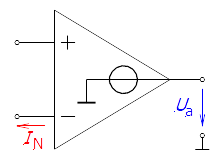
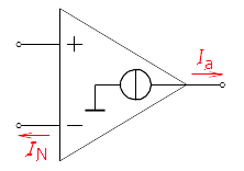
As seen in Figure 2.1, a Biquad Filter consists of four Operational Amplifiers. To get a better understanding of these, this chapter will discuss the main aspects of OPAMPs. There are different types of operational amplifiers that differ, for example, by their low- or high-impedance inputs and outputs. According to Schmid, there exist nine different types of the Opamps, but only four are mainly used (Schmid 2000). This is because almost always, the non-inverting (positive) input is designed as a high-impedance voltage input. The inverting (negative) input can either be a high-impedance voltage input or a low-impedance current input, depending on the type. Accordingly, the output can be either a low-impedance voltage output or a high-impedance current output. This results in four basic configurations, as shown in the accompanying table Table 2.1. (Images are taken from Wikipedia (2025))
| Voltage output | Current output | |
|---|---|---|
| Voltage input | Voltage-Feedback Amplifiers | Operational Transconductance Amplifier |
 |
 |
|
| Current input | Current-Feedback Amplifiers | Current Amplifier |
 |
 |
As a general rule, the simplest circuit that can do a job is usually the best choice. (H. Pretl and Michael Koefinger 2025)
2.2.1 Voltage-Feedback Amplifiers (VFA)
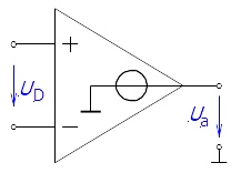
When discussing operational amplifiers (OPAMPs), most sources refer to the Voltage-Feedback Amplifier. These VFAs are voltage-controlled voltage sources, essentially acting as voltage boosters. They are characterized by a high-impedance input for both the non-inverting and inverting terminals, and a low-impedance voltage output. To realize various desired circuits, such as amplification, integration, addition/subtraction, etc…, these functions should ideally be achieved only through the surrounding circuitry. To meet this requirement, three main requirements need be satisfied:
- Extremely High Voltage Gain: Typically ranging from 60 to 120 dB (or gain factor of \(10^4\) to \(10^6\)), this gain should be available over a wide frequency range.
- High Impedance at Differential Inputs: Ensuring minimal loading of the signal source.
- Low Impedance at the Output: Allowing the amplifier to drive various loads without significant voltage drop.
Voltage source
A voltage source creates a constant voltage output by changing the current.
Current source A current source creates a constant current by changing the voltage.
Both of this sources can be explained by Ohm’s Law: \(R = \frac{U}{I}\).
For example the voltage source: There is no influence of the load, so \(R\) may change and its value is unknown to the source. So to keep the voltage stable we can only change the current.
2.2.2 Operational Transconductance Amplifier (OTA)
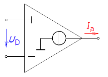
In the design process of the biquad only OTAs will be used, so the focus of this chapter will be on them. The operational transconductance amplifier puts out out a current proportional to its input voltage, unlike Voltage Feedback Amplifiers Section 2.2.1. In other words, an OTA is a voltage controlled current source.
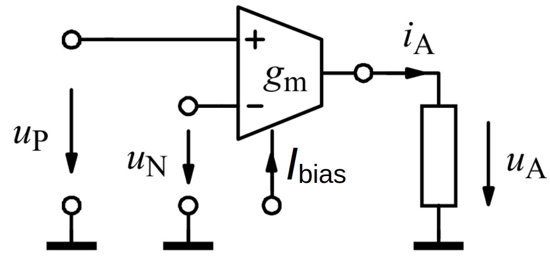
As seen in the figure Figure 2.3, the OTA has the two differental inputs and a current output. On top of that it has a biasing current input \(I_{bias}\) which controls the transconductance \(g_m\) of the OTA.
2.2.2.1 Transconductance
Transconductance is a fundamental parameter that describes the relationship between the input voltage and the output current in electronic devices, particularly in transistors. It is defined as the ratio of the change in output current to the change in input voltage, under conditions where all other variables are held constant. Mathematically, it is expressed as:
\[ g_m = \frac{\Delta I_{out}}{\Delta V_{in}} \]
where \(g_m\) is the transconductance, \(\Delta I_{out}\) is the change in output current, and \(\Delta V_{in}\) is the change in input voltage. The unit of transconductance is the siemens (\(S\)), which is equivalent to amperes per volt (\(A\)/\(V\)). Historically, it was also measured in “mho”, which is “ohm” spelled backwards, reflecting its inverse relationship to resistance.
In field-effect transistors (FETs) the transconductance determines the device’s ability to amplify signals. A higher transconductance value indicates a stronger amplification capability, as a small change in input voltage can result in a significant change in output current.
The term transconductance originates from the concept of transfer conductance. It combines the ideas of transfer, indicating the transfer of a signal from the input to the output, and conductance, which is the inverse of resistance and measures how easily a material conducts electric current. In essence, transconductance describes how effectively a device can convert a voltage change at its input into a proportional current change at its output. Kids (2025)
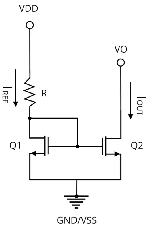
2.2.2.2 5-Transistor OTA
H. Pretl and Michael Koefinger (2025) introduces a basic 5-Transistor OTA as a design proposal for a real circuits.
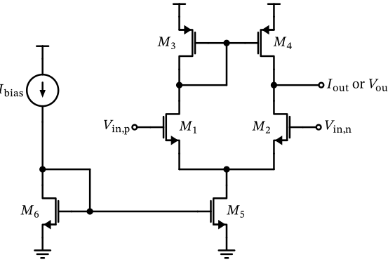
It consists of few elements which are going to be described in the next chapters. The basic function of this OTA can be described with: The transistors \(M_1\) and \(M_2\) form a differential pair, which is biased by the current source \(M_5\). Transistors \(M_5\) and \(M_6\) create a current mirror, where the input bias current \(I_{\text{bias}}\) sets the bias current for the Operational Transconductance Amplifier. To keep the biasing current stable, a current mirror (Section 2.2.3) is used instead of applying the \(I_{\text{bias}}\) directly to \(M_5\). The differential pair (Section 2.2.4) \(M_1\) and \(M_2\) is loaded by the current mirror \(M_3\) and \(M_4\), which mirrors the drain current of \(M_1\) to the right side of the circuit. The combined currents from \(M_4\) and \(M_2\) at the output node result in the generation of an output current. To achieve this desired result, it is important to ensure that \(M_{1,2}\) and \(M_{3,4}\) are symmetric, meaning they should have identical \(W\) (width) and \(L\) (length) dimensions. To set the right bias current, \(M_{5,6}\) should be chosen accordingly.
2.2.3 Current Mirror
A current mirror consists of at least two transistors, one working as the input (reference) source and the other ones as copies of it. As the name suggests, the primary function of a current mirror is to copy the input current to the output, ensuring that the output current is an exact duplicate of the input. Importantly, the flow of the input current is unaffected by the size of the mirrored output current or any variations in it.
This behavior is made possible by two key characteristics of the current mirror: its relatively low input resistance and its relatively high output resistance. The low input resistance ensures the input current remains stable regardless of drive conditions, and the high output resistance maintains a constant output current independent of load variations. (Analog University (2024))
A current mirror is also capable of copying one current and converting it to multiple different outputs. This is possible by attaching more transistors with their gate \(G\) to the drain \(D\) of the reference transistor. By scaling the width and length of each output transistor differently, multiple scales of the input current can be created. Hereby, a big advantage is when using MOSFETs, due to the fact that no current is flowing through the gate. In the case of BJTs, a compensation circuit is added. (H. Pretl and Michael Koefinger (2025))
2.2.4 Differential Pair
A differential pair, also referred to as a differential amplifier, is an electronic circuit designed to compare the difference between two input voltages while minimizing any voltage that is common to both inputs. It consists of two transistors and can have two inputs and two outputs, as seen in Figure 2.6.
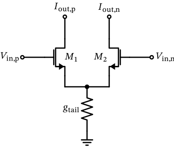
Its primary function is to amplify the difference between two input signals while rejecting any common-mode signals, which are identical in both amplitude and phase at the two inputs. This property makes the differential pair highly effective in noise reduction and signal processing applications. In a typical differential pair using MOSFETs, the two transistors are matched in terms of their electrical characteristics, such as threshold voltage \(V_{th}\) and transconductance \(g_m\). The inputs are applied to the gates \(G\) of the MOSFETs, while the outputs are taken from the drains \(D\). A current source is usually connected to the sources \(S\) of the MOSFETs to provide a constant bias current, here noted as \(g_{\text{tail}}\) or like in Figure 2.4 as \(I_{\text{bias}}\).
The differential gain of the pair is determined by the transconductance \(g_m\) of the MOSFETs. The common-mode rejection ratio (CMRR) is a measure of the differential pair’s ability to reject common-mode signals. It is defined as the ratio of the differential gain to the common-mode gain and is typically expressed in decibels (dB). The performance of the differential pair is also influenced by the tail current source, represented by \(g_{\text{tail}}\). The tail current source provides a constant bias current \(I_{\text{bias}}\) that flows through both transistors, ensuring that the total current through the differential pair remains constant regardless of the input voltages. (Razavi (2024))
When used in OTAs, the differential pair serves as the input stage, where the differential input voltage is converted into a differential current.
2.3 MOSFET (Metal-Oxide-Semiconductor Field-Effect-Transistor )
To dive in one more level, the parts an operational amplifier is build of are transistors. Precisely in this design process they are (MOSFETs). In integrated circuit design, where pre-built components are not available, MOSFETs can be designed from scratch. This design flexibility allows for the adjustment of the MOSFET’s physical dimensions, specifically its width \(W\) and length \(L\). By doing this there is a lot of room for freedom and experimental space. The length \(L\) significantly influences MOSFET performance, enabling a trade-off between speed and output conductance. The width \(W\) of a MOSFET acts as a scaling factor that adjusts the charge density within the channel, enabling the control of current levels to meet specific design requirements.
In the literature, the circuit symbol of MOSFETs is not uniform. Some denote them with a small arrow between the gate (\(G\)) and source (\(S\)), which is not very precise due to the fact MOSFETs are symmetric. This means that the drain (\(D\)) and source (\(S\)) can be interchanged, and the names are only defined to make circuits clearer. Therefore, an accurate symbol for the n-MOS (shown in Figure 2.7) and p-MOS (shown in Figure 2.8) is shown in the following figures taken from H. Pretl and Michael Koefinger (2025):
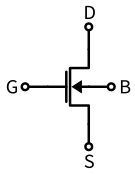
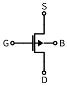
However, in this development report, the symbols are not strictly used like shown here. But all of the used figures are based on this symmetric model of a MOSFET.
Besides, in many situations the bulk \(B\) is connected to the source \(S\) terminal. Thus the bulk \(B\) is not mentioned in the circuit diagrams.
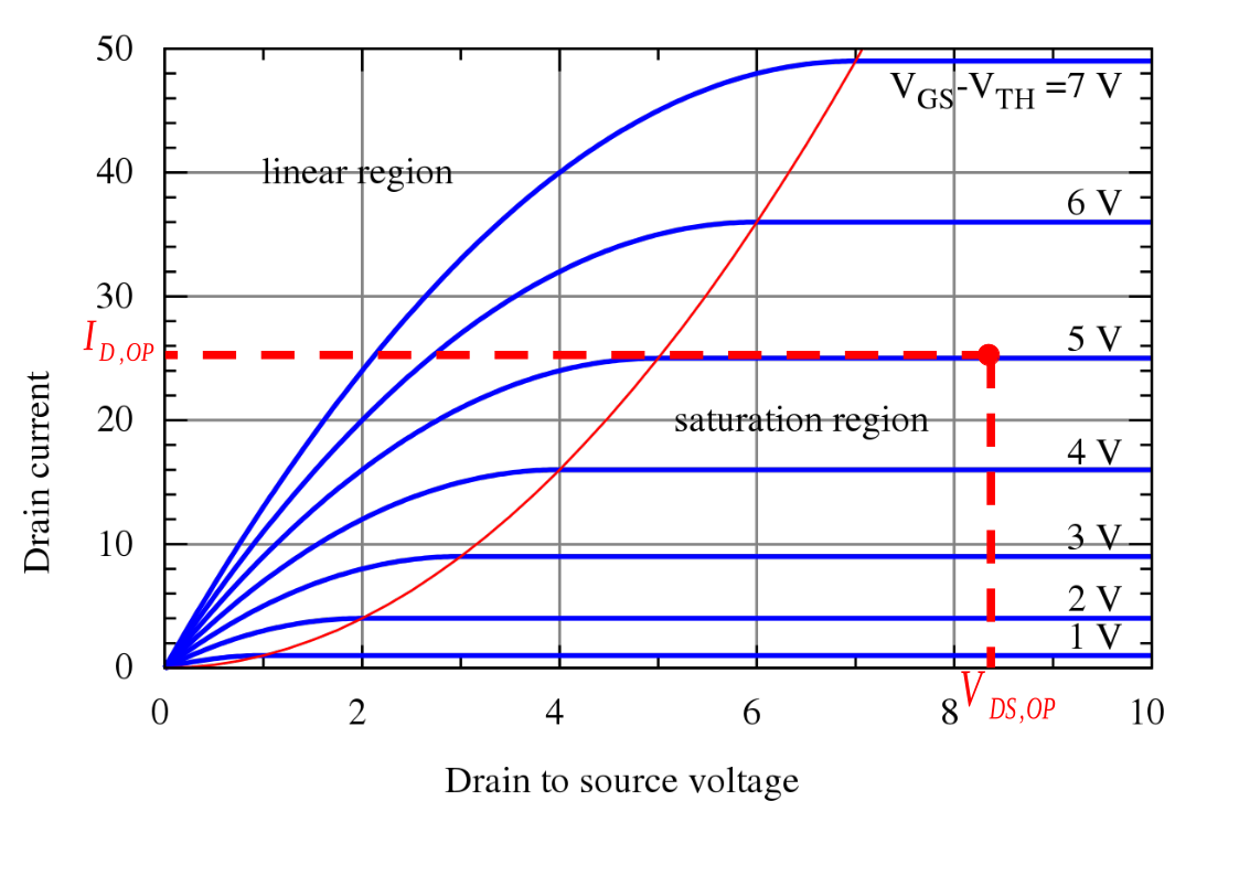
2.3.1 MOSFET Large-Signal Regions
A MOSFET can operate in three different modes: Saturation, Linear (or Triode) region, or Cutoff. The modes depend on the device’s threshold voltage \(V_{\text{th}}\), gate-to-source voltage \(V_{\text{GS}}\), and drain-to-source voltage \(V_{\text{DS}}\).
Saturation
The saturation region is the active mode used for analog amplification, where the MOSFET behaves like a voltage-controlled current source. A conductive channel forms between the source and drain. This state is reached when the condition \(V_{\text{DS}} \geq (V_{\text{GS}} - V_{\text{th}})\) is met. In saturation, the drain-source current (\(I_D\)) stabilizes or “saturates” and becomes nearly independent of \(V_{\text{DS}}\). However, it can still be precisely controlled via \(V_{\text{GS}}\) due to the phenomenon known as “pinch-off”.
Linear Region
The Linear, or Triode, region occurs when a MOSFET is conducting and acts more like a resistor or voltage-controlled device rather than a current source. This region is defined by the condition \(V_{\text{DS}} < (V_{\text{GS}} - V_{\text{th}})\) and \(V_{\text{GS}} > V_{\text{th}}\). In this mode, both \(V_{\text{GS}}\) and \(V_{\text{DS}}\) control the \(I_D\), allowing the device to be used effectively for switching and amplification in low-voltage applications.
Cutoff Region
In the cutoff region, the MOSFET is effectively turned off, with no conductive channel formed between the drain and source. This mode is reached when the gate-to-source voltage is less than the threshold voltage (\(V_{\text{GS}} < V_{\text{th}}\)). In cutoff, the drain-source current \(I_D\) is nearly zero, which means the MOSFET is not conducting and behaves like an open switch.
In the large-signal analysis, the transitions between operating modes occur gradually, making it challenging to pinpoint an exact moment when one mode shifts to another. Consequently, the modes are used in a more approximate manner, reflecting the continuous nature of these transitions rather than distinct, sharply defined states.
2.3.2 Small-Signal Representation
By applying different voltages to a MOSFET, different behaviours appear. But there is one thing which is very unliked by engineers and others, all these transfer functions are non linear. So making any calculations by hand is nearly impossible. That’s why in practise the biasing method exists. This is done by applying a dc voltage to the terminals of the MOSFET and during operation only a small signal change appears. With this technique an Operating Point is created, which enables to assume a linear behaviour in its small signal area (like in Figure 2.9). Because the MOSFET is put into an small operation point and all the changes applied are very small, this linearisation area is called Small-signal model.
- \(I_D\): The drain current
- \(I_{\text{bias}}\): The biasing current. The current to adjust the operating point
- \(V_{GS}\): The gate-to-source voltage
- \(V_{DS}\): The drain-to-source voltage
- \(V_{th}\): The threshold voltage. A critical parameter that defines the minimum gate-to-source voltage \(V_{GS}\) required to form a conductive channel between the source and drain
- \(V_{OV}\): The overdrive voltage. the difference between the gate-to-sourcevoltage \(V_{GS}\) and the threshold voltage \(V_{th}\).
- \(g_m\): The transconductance. The ratio between the output current and input voltage
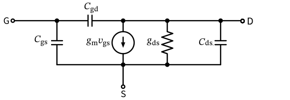
2.3.2.1 Capacitances in MOSFETs
Gate-Source Capacitance (\(C_{gs}\)):
\(C_{gs}\) is the capacitance between the gate and source terminals. This arises due to the physical overlap of the gate and source regions, as well as the insulating oxide layer between them. \(C_{gs}\) affects both the input impedance and the switching speed. Higher \(C_{gs}\) values can slow down the switching process because more charge needs to be moved to change the gate voltage.
Gate-Drain Capacitance (\(C_{gd}\)):
\(C_{gd}\) is the capacitance between the gate and drain terminals. People also know it as the Miller capacitance because of its significant impact on the Miller effect. The Miller effect amplifies the effective value of \(C_{gd}\), making it a critical factor in determining the high-frequency behaviour of the MOSFET. This capacitance can cause phase shifts and affect the stability of the circuit, particularly in amplifiers.
Drain-Source Capacitance (\(C_{ds}\)):
\(C_{ds}\) is the capacitance between the drain and source terminals. It arises due to the depletion region between the drain and source regions. \(C_{ds}\) affects the output impedance and frequency response of the circuit. Higher drain-source capacitance can lead to increased output capacitance, affecting the switching speed and introducing additional losses.
2.3.2.2 Transconductances in MOSFET
Output Conductance (\(g_{ds})\)
\(g_{ds}\) represents the small-signal conductance between the drain and source terminals of the MOSFET. It expresses how the drain current \(I_D\) changes with respect to the drain-source voltage \(V_{ds}\) when the gate-source voltage \(V_{gs}\) is held constant. Mathematically, it is defined as follows:
\(g_{ds}=\frac{\partial I_D}{\partial V_{ds}}\bigg|_{V_{gs}=\text{constant}}\)
\(g_{ds}\) affects the output impedance of the MOSFET. A higher \(g_{ds}\) results in a lower output impedance.In saturation region, \(g_{ds}\) is typically small, which helps maintain the linearity of the device. However, in the triode region, \(g_{ds}\) can be larger, leading to non-linear behaviour.
Mutual Transconductance - Gate-Source Voltage (\(g_mv_{gs}\))
The transconductance \(g_m\) of a MOSFET quantifies how the drain current \(I_D\) varies in response to changes in the gate-source voltage \(V_{gs}\), while keeping the drain-source voltage \(V_{ds}\) constant:
\(g_m=\frac{\partial I_D}{\partial V_{gs}}\bigg|_{V_{ds}=\text{constant}}\)
The term \(g_mv_{gs}\) represents the small-signal current generated by the transconductance \(g_m\) in response to a small change in the gate-source voltage \(v_{gs}\). A higher \(g_m\) results in a higher voltage gain.
In the saturation region, the output conductance \(g_{ds}\) is generally much smaller than the transconductance \(g_m\). This characteristic enables the MOSFET to function effectively as a voltage-controlled current source. However, as the MOSFET moves into the triode region, \(g_{ds}\) increases, causing the device to behave more like a resistor. The output conductance \(g_{ds}\) influences the output impedance and linearity of the device, while the product \(g_mv_{gs}\) controls the gain and frequency response of the circuit.