5 Integrated Layouting
The following chapters describe how to design an integrated circuit using the software KLayout. An introduction and setup for the software will be given as well as some tips and tricks to easier work with the software.
5.1 Introduction into the fundamentals of integrated layouting.
Before designing on the wafer, the basics of the design process must be understood. To that end an explanation of the software as well as the physical layers is necessary to comprehend the design challenges.
When designing an integrated chip, the designer first needs to choose a technology. Each technology has different design rules and properties, which makes it suitable for the application. A technology usually comes with a process design kit (PDK). A PDK contains a device library, verification checks and technology data.
The device library contains the symbols used in the schematic and the PCells/devices used in the layout. The verification checks consist of the design rule check (DRC) as well as the layout vs. schematic (LVS). The technology data represents the basis of DRC and defines the physical constraints of the technology (see Wikipedia contributors (2025))
The used technology was the sg13g2 technology from IHP. Which is a BiCMOS technology with a 130nm minimum gate length. This PDK is open source and in a preview status (see IHP‑GmbH (2025a))
To design the layout itself one first needs to be familiar with the different masks and the structure of a waver. The following is a simplified explanation of the different layers, their use and the manufacturing process behind it. For this report this is kept simple and will only focus on the layers used in the design. The simplified explenation was heavily inspired by the chapters 2 to 5 in CMOS by Jacaob Baker (see Baker (2010)).
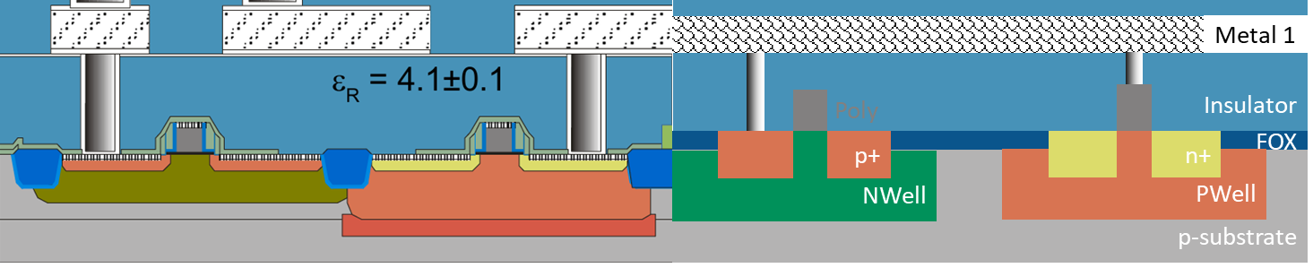
The base is the bulk and a field oxide (FOX) layer on top of it. In this technology the bulk is a p-substrate. The FOX layer is an insulator, which separates devices from one another.
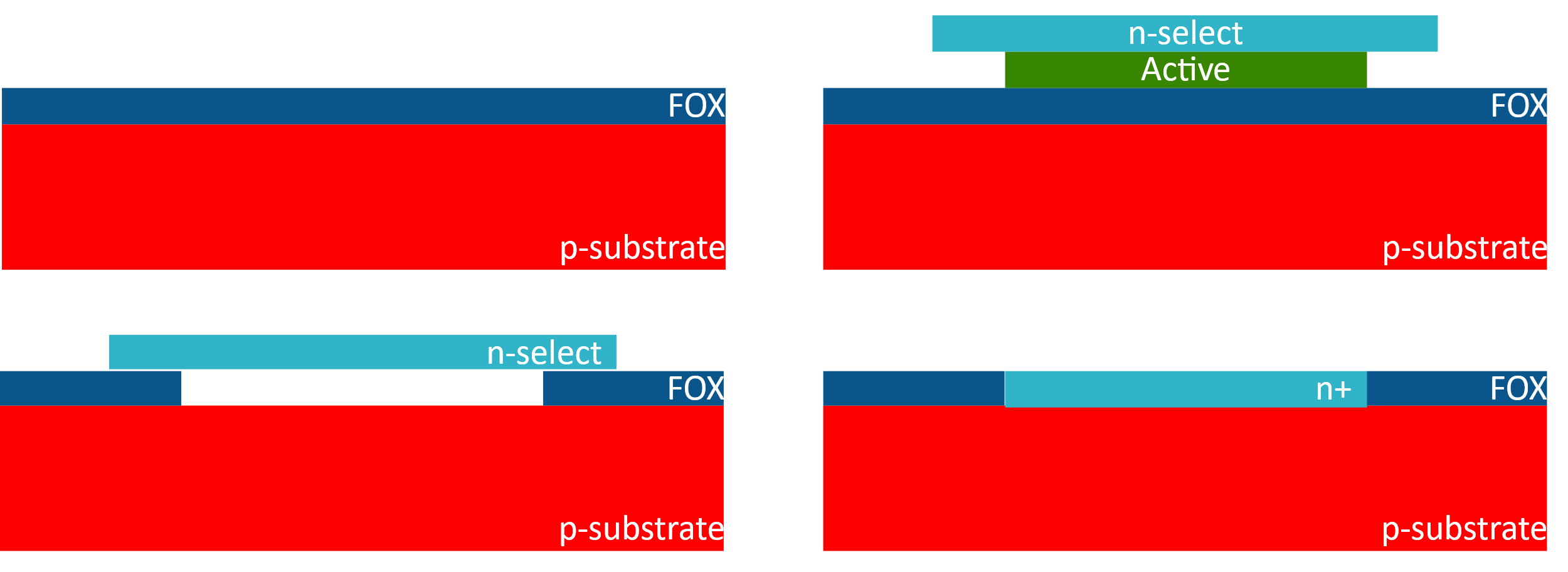
To make a device first the FOX layer needs to be opened (see Figure 5.1). That is done by etching away the FOX. The active mask allows the designer to specify the areas where the FOX will be opened. This is necessary for the doping process, which is usually done by an n- or p-select mask. In sg12g2 the n-select mask does not need to be specified. It is necessary to remove the FOX, otherwise the doping specified in the n-select mask will be stopped by the FOX. The select mask also needs to be bigger than the Active mask due to misalignment during the manufacturing process.
The next layer is the poly layer. The poly layer forms the gate of the transistors, the name is an abbreviation for Polysilicon. The poly can be routed like normal metal layers, with the exception that it is for more restive than the metal layers, so caution is advised for long poly traces.
In the manufacturing process the thick poly layer prevents the n-select mask to dope the part below the gate, therefore creating the drain and source regions of the nmos (see Figure 5.2).
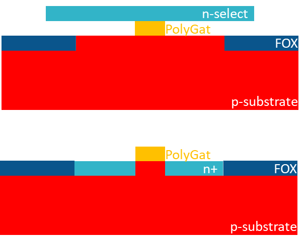
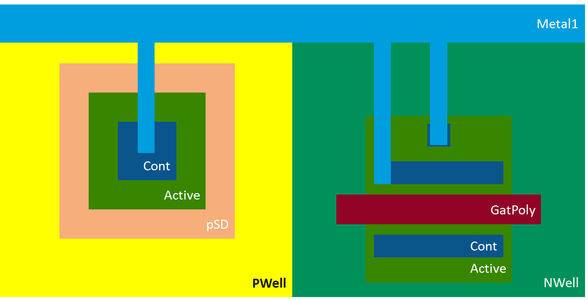
Also note that the drain and source contacts are interchangeable, as they are identical regions in the active area. The last two pictures showed how an NMOS device is formed. As mentioned before, the n-select mask doesn’t exist in the used PDK, but the p-select mask does exist with the label pSD.
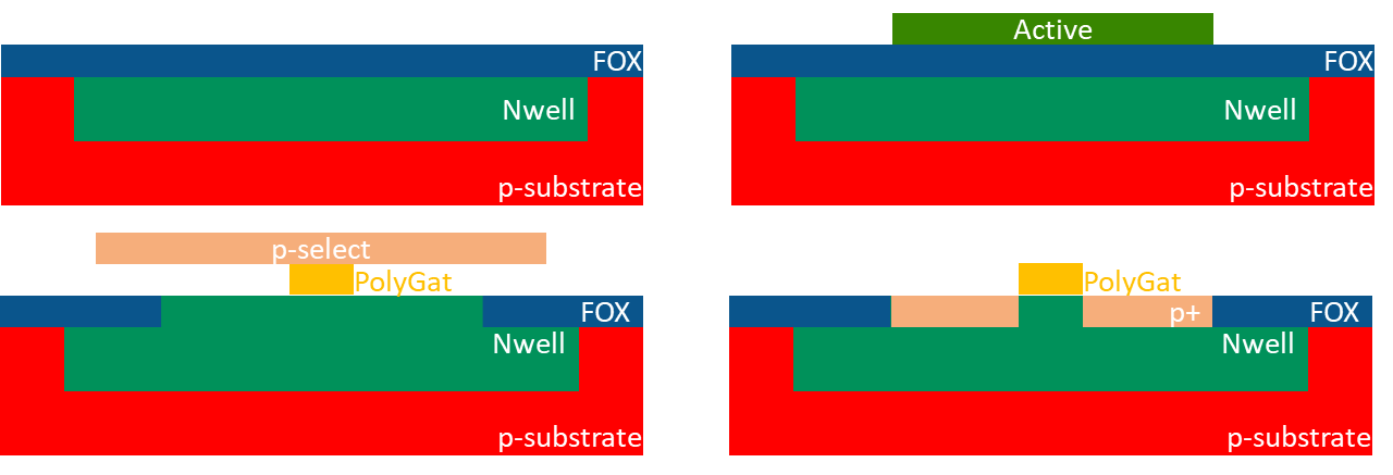
As the PMOS is a negated NMOS, the designer first needs to place the p+ regions in an n-substrate. This is done by enveloping the transistor in an NWell. The NWell is a region that can be specified by the designer and works like an implant in the substrate. The FOX is also opened by the active layer but pSD layer is used to implant the p+ region (see Figure 5.3).
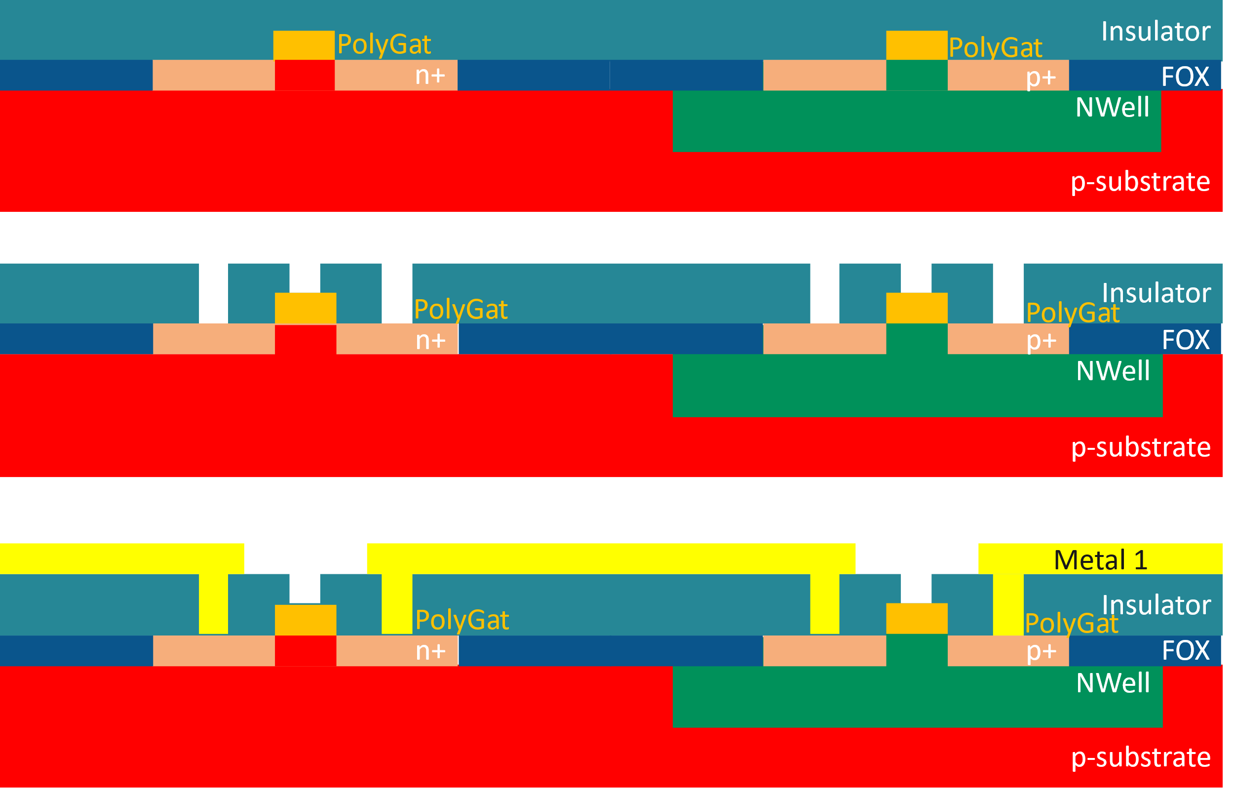
The N- or PMOS is formed in the bulk, but there are no electrical connections to the pins of the device. Connections between devices can be established using the poly or active layer, but both options are not advised. Therefore, the first metal layer is used for connections between devices. Connections from an active or poly layer region to the metal layer can´t be made by overlaying the layers as they are separated by an insulator. To connect these different layers the contact layer (Cnt) is used. It connects active or poly layer to the metal 1 layer, by removing the insulator over these regions (see Figure 5.4). Note that the first connection between these regions is always over the metal 1 layer. To switch between the different Metal layers, vias can be used, similar to a multilayer PCB design. These vias are formed by opening the insulator and placing in an conductor like tungsten the opening. In the figure this process is simplied.
The MOSFET is a 4-pin device, consisting of source, gate, drain and body. While the body often is omitted on a schematic level, in the integrated layout the body of the MOSFET need to be tied to a defined potential. The body is also called the substrate or bulk, in case of a PMOS it is the NWell.
For the nmos this means connecting the substrate to VSS, while the NWell of a PMOS will be pulled to VDD. To have multiple locations to where the bulk or NWell connected to their potentials is advised.
The later chapters will work in the sg13g2 technology, the knowledge acquired in this chapter can be mapped to this technology. The figure (see Figure 5.5) compares the technology on the left, with the learned knowledge on the right. Note that the PWell is not used for NMOS devices only for ties.
5.2 KLayout
The previous chapter described the fundamentals of the integrated layout, in this chapter these fundamentals are put into practice to create the layout for the 5T-OTA outlined by the schematic by Haraled Pretl(see Pretl et al. (2025))
The schematic outlined by Professor Pretl consists of 13 N- and PMOS devices. These devices are defined within the PDK and are the fundamental blocks, which make up the layout within the technology. Within the layout software these are defined as PCells. As the schematic designer works out the optimal design, one of the main variables to change the behaviour of the MOSFETs, is the w/l ratio. This ratio defines the width and length of the gate over the active area. These w/l ratios are crucial to the layout process, as they define the physical size of the devices. In the layout the w/l values were given by the calculation of Professor Pretel. These w/l ratios will be used to configure the PCells.
The layout program used is called KLayout. Similar to Xschem it works in a strict hierarchical system. As the layout of the 5T-OTA will be used in the Top-Level layout of the Biquad, the 5T-OTA itself is a cell, that can be called multiple times, throughout the layout of the Top-Level. To make it easier for the designer to connect the individual components of the Top-Level together, the 5T-OTA just uses the metal 1 layer. The interface points are the vias stacks. Therefore, making connections on the higher layers easier, as the individual cells for the 5T-OTA only reside on the most bottom layer.
In the following chapters DRC and LVS will be important concepts. DRC (Desing Rule Check) describes the process of comparing the physical layout to the constrains of the technology. This will throw an error, for example if a “trace” on the Metal1 layer is too thin. LVS (Layout Versus Schematic) describes the process of comparing the schematic to the layout. This will throw an error when two nets are shorted or a device it not correctly connected.
5.2.1 The Setup of KLayout
While the previous chapters showed only a cross section of the waver, the designer only sees the waver from a top view, but needs to recall the cross section, while working on the layout. This especially true for the layer that can be used as conductors.
This chapter will explain how to set up KLayout and the tools necessary to run DRC and LVS. It also shows an example way for a simple workflow.
Before the layout process begins it is paramount aggravate all the data files necessary. To do that create a new folder labelled Layout and copy your schematic design into this folder. Consider renaming your schematic into letters only. Do not use special character similar to UNIX symbols, only underscores are permitted.
To create a valid netlist, open the schematic in Xschem. Under simulation->LVS make sure that “LVS netlist + Top level is a .subckt” and “Upper case .SUBCKT and .ENDS” is selected.
After selecting these options, run the netlist and simulation. In the folder structure a new folder labelled simulations with file named “YOUR_PROJECT.spice” should appear. Copy that file into your main layout directory.
To begin designing create a new layout file called the same as the schematic by running “Klayout -e”. The argument -e opens Klayout in editing mode. To make the editing mode default, select File->Setup->Application->Editing Mode->Use editing mode by default.
To create a new layout, select “New Layout”. A wizard should appear that allows the selection of the technology. It is important to rename the Top Cell to match the name of your schematic so “YOUR_PROJECT”.
Please note that all the scripts later used are case sensitive, so consider this when renaming files.
Upon first saving, select the GDS file standard and name your file YOUR_PROJECT.GDS. The main layout directory should now contain YOUR_PROJECT.sch/.spice/.gds files. As well as a simulation folder. Now create a folder called LVS in this main layout directory.
For ease of access, create shell-script in your main layout folder to run LVS. The command saved with in the file should be:
python /foss/pdks/ihp-sg13g2/libs.tech/klayout/tech/lvs/run_lvs.py --netlist=YOUR_PROJECT.spice --layout=YOUR_PROJECT.gds --run_dir=LVS/Try running this command, to ensure it runs correctly. If it fails, saying something about “use_same_circuit”, check the names of your files, including the cell name of your layout. It’s crucial that all files are named the same.
This script will produce a. lvsdb file in the LVS directory. This file contains the comparison between the netlist of the schematic, as well as the extracted netlist of the layout.
As the design process is a constant back and forth with design and running LVS and DRC, these steps are necessary to ensure a good workflow.
Before designing we need to set up the tools in Klayout. For the DRC, open Macros->Macro Development and select DRC->[Technology sg13g2]->sg13g2_maximal. Copy the contents of this script and paste them into a new DRC script. Running this script will provide the “Marker Database Brower” from which the individual DRC errors can be selected. As the error names and a semi-detailed description can be found the “SG13G2_os_layout_rules.pdf” on the Github of IHP (see IHP‑GmbH (2025b)).
To run LVS run the shell script and open the netlist browser under Tool->Netlist Browser. To see the LVS errors click on file->open and then navigate to /LVS/YOUR_PROJECT.lvsdb. This only needs to be done one time, as the LVS shell script will override the current .lvsdb file, when run anew. Select File->Reload to get the current LVS-data.
After loading the .lvsdb file the cross-reference tab will show the discrepancies between the netlists. This is because no layout has been created yet.
To provide a better overview of the used layers, right click on the right-hand side layer tab to open a pop up menu and select “hide empty layers”.
Disabling navigation by holding the middle mouse button: Check File->Setup->Navigation->Zoom and Pan->Mouse alt mode. This allows the control more similar to Autodesk Fusion or KiCad.
Disabling the zoom when pasting: File->Setup->Navigation->Zoom and select Pan->On paste->Pan to pasted objects. This option disables the full zoom to object, which can cause disorientation.
To show all the hierarchy and layers select Display->Full Hierarchy
To change to dark mode select File->Setup->Display->Background->Background Color->#42
The real layout process can now begin in Klayout. Different from PCB design, the symbols on the schematic side do not need to be matched to a footprint. Rather the symbol are the fundamental devices in the technology. To work with the devices of the technology open the library on the down-left under Libraries->SG13_dev. The list below shows the usable devices. By dragging and dropping them into the design, the devices are placed in the layout.
In previous chapters mentioned the w/l ratios will now play a role as the individual devices are configured. To configure a device or PCells, double click it and navigate to PCell parameters and enter the W/L ratios. Updating the PCell will change the device to the desired parameters.
5.3 The Layout Process
The workflow is much more incremental than in PCB design, as one implements device by device.
To that end, it is practical to copy the original schematic and delete the already placed devices, to maintain an overview of the progress. After every two to three cells, it is advised to run LVS and DRC.
Placing and configuring a device was already described, connecting devices is usually done by the Metal1 layer. It is advised to work with the metal layer alongside the hierarchy. So for the top level use the higher metal layers like Metal3 to Metal6, while for the lower levels use Metal1 to Metal2.
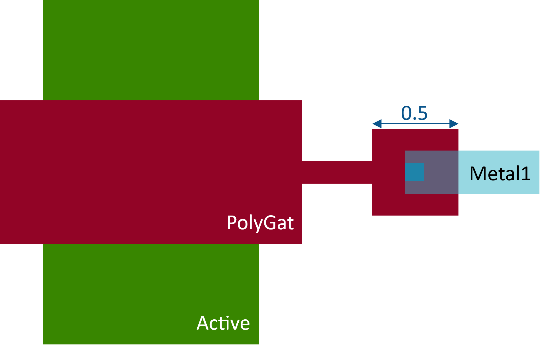
To connect different pins, use the LAYER.drawing layer. Conductors can either be the GatPoly or the Metal layers. Keep in mind that GatPoly.drawing has a higher resistance that Metal.drawing. To switch between the metal layers, use the device called “via_stack” and configure it accordingly.
To connect the gate of a MOS device the GatPoly needs to be connected to Metal1 through the Cnt layer. In contrast to the source and drain contacts this need to be done by hand. See (Figure 5.6) for a DRC clean connection of the gate of an NMOS device.
In general, connect each device separately from each other. It might be tempting to design the layout close together, with overlapping NWells, Active and GatPoly areas, but this will lead to both DRC and LVS errors, which will be difficult to address as each device is close together. This is especially true, when first learning the process.
The layout of the 5T-OTA was done in multiple iterations, each iteration taught valuable lessons. The next section presents these lessons, outlining a specific workflow and offering tips and guidance for beginners.
Run LVS and DRC every 1 to 3 devices!
Aligning structures is easier when using a crosshair.
Enable this by checking View->Crosshair CursorUse the path tool whenever possible.
The tool has an adjustable width, which can be set on the bottom right menu.
Set this width to 0.16 um to route DRC free on most layers.
Do not use free form, as jagged shaped will create DRC errors.
Use the shift key to snap to constrain vertically or horizontally.
To change the layer of structure, select the desired layer, select the structure and press shift+L
Copying and pasting a structure will result in duplicating the structure in place. Use the move tool to separate both structures.
If things get too cluttered use the layer menu to declutter the interface.
Right clicking and selecting “Visibility follows selection” will only show the selected layer.
Setting different tabs for routing, DRC checking or overviewing the general layout is a good option to keep things tidy and readable
Changing the appearance of different layers is a good idea, especially for layers that overlap, like pSD or NWell.
Use the polygon only on special occasions as it is harder to clear of DRC errors.
The devices will not be placed automatically.
There is no way of changing the grid, as it is defined in technology.
There is no “Ratsnest” or “Airal Connections”.
There is no DRC in the background, short circuits will only be caught by running the LVS.
There is no net highlighting.
There are no zones, but their absence will cause DRC errors.
There is no dragging, moving a device always means moving the “traces” by hand with it.
There are no footprints, the PCells are the fundamental footprints defined by the technology.
Text size can’t be set but will adjust to the zoom level.
The GUI is sometimes not working, especially true for LVS.
5.3.1 Working with LVS during layouting
The Netlist Database Browser will provide an overview of all the nets both in the layout and the schematic or “Reference”. Each net has a number in brackets behind it. This number describes all the pins it is connected to. The netlists will only then match if these numbers are matched.
During the layout process it is paramount to use the LAYER.text layers and the text tool to assign labels to the GatPoly or Metal1 layers. To select these layers, one may need to show all layers under Layer->Show all. To keep the comparison in the netlist browser simple, name the nets of the layout according to the names of the nets in the schematic. Please refer to the designer’s etiquette, while labeling the layout or schematic (see Pretl, Koefinger, and Dorrer (2025)).
When working out the LVS it is advised to check mainly the devices in the list. This will provide a comprehensive overview of the devices, and the nets connected to them. Running LVS and DRC frequently will help with the overview.
It is normal that even the correctly wired devices are shown as errors. Especially the drain and source pins often swap places, which can’t be fixed by rotating the device. To clear the errors all nets connected to the device need to be cleared first. Only when all nets are correctly connected, will the device be clear of errors.
Having two nets on the same pit is always short circuit and should be handled with the highest priory.
After a few MOS devices are placed, LVS will throw an error as their body “pin” is not connected to a defined potential. In an prior chapter the process of tying down the substrate was already explained. In this technology the substrate is a p-substrate, this means the NWells need to be tied down and there must be multiple tying down points for the p-substrate (see Figure 5.7). Please note that the size of the masks shown has been altered for visibility reasons. Also note that each PMOS needs its own tie to the VDD potential, while the ties for the NMOS can be placed anywhere on the layout, as the substrate is the bulk.
While using the netlist browser allows also for a rudimentary net highlighting in the layout. The practicality depends on the number of devices connected to the net. In general troubleshooting get more difficult, the more pins are connected to the same net.
5.3.2 Working with DRC during layouting.
Running the DRC often and addressing them as soon as possible, allows for a denser and generally more compact layout. It also reduces the time spend reworking the layout after all devices have been connected.
As described in set up chapter the “Marker Database Browser” is a built-in tool for addressing DRC errors. This tool shows the amount of DRC errors as well as the type. After following the steps described in the setup, one can open the Brower under Tool->Marker Browser. And running the DRC by selecting the run button.
The DRC will categorise in cells. Opening the DRC error log up will show the name of the error. Names link to the “SG13G2_os_layout_rules.pdf” by IHP. While KLayout also provides a description of the errors, it is best to use the DRC in conjunction with the DRC-PDF. The DRC-PDF provides context and dimensions for each error.
Working dually with the DRC-PDF and the DRC-Browser, allows the user to first clarify the DRC errors and than locate it by selecting it in the browser.
A very useful tool to clear DRC errors is the “partial” tool in the toolbar. This allows to modify structures after they are placed. This speed up the workflow immensely as the structures don’t need to redrawn.
Some DRC errors can’t be fixed at a given point of the design process. These DRC errors are usually due to density errors. But as the layout is not fully completed, cleaning these DRC errors has at best no impact on the design. Nevertheless, these errors must be cleared before the tape out.
5.4 The layout of the 5T-OTA
To design the 5T-OTA the schematic and the values of Professor Pretel were used (see Pretl et al. (2025)).
As the export functionality of KLayout is rather limited, it is best to open the .gds file in KLayout directly, but the is also a SVG in the layout folder.
While not very space efficient the layout followed the location of the MOSFETS in the schematic to ensure readability. This helped during the layout process, as it gave a clear structure to the layout. This also benefitted the understanding of the LVS and DRC during the layout immensely.
As space is one of main drivers of cost in IC design, a final version should be more mindful of the space used by the devices and traces. This would also clear the density errors, due to a higher density, because of the more compact design.
The design features multiple NWell and PWell Ties, to ensure that both bulks and NWell are connected to their potentials. Each PMOS-device has and NWell tie, which is closely located to the device. The PWell ties surround the design, as described in the introductory chapter to the integrated layout, the bulk shares one potential, but it is good practice to not use a star formation, to ensure this potential is evenly distributed.
One of the design goals of the design is the connection only on the first metal layer, this should ensure that the connection layers above are not influenced by the design. In addition, it provides a clear connection point for the top-level schematic.
The 5T-OTA.gds could easily be imported as cell into an arbitrary top- or mid-level design. Which concludes the design goal of this report.